Suheng Xu
Graduate research assistant@ Columbia University in the City of New York
Department of Physics, Columbia University
Biography
I am a PhD candidate in the Physics Department at Columbia University, working in experimental condensed-matter physics. I develop and apply advanced imaging approaches to visualize quasiparticles and collective excitations in space and time.
-
BSc in Physics
Jilin University, China
-
PhD candidate in Physics
Columbia University, USA
Featured Publications
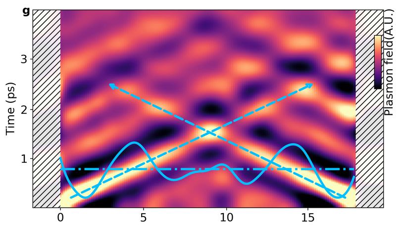
Plasmons are collective oscillations of mobile electrons. Using terahertz spacetime metrology, we probe plasmon dynamics of mono- and bi-layer graphene. In both systems, the experimentally measured Drude weight systematically exceeds the prediction based on non-interacting electronic system. This enhancement is most pronounced at ultra-low carrier densities. We attribute the observed deviation to pseudospin dynamics of the Dirac fermions in multi-layer graphene, which leads to a breakdown of Galilean invariance. Our results establish that pseudospin structure of the single-particle electronic wave function can directly govern collective excitations, with implications that extend beyond graphene to a broad class of quantum materials.
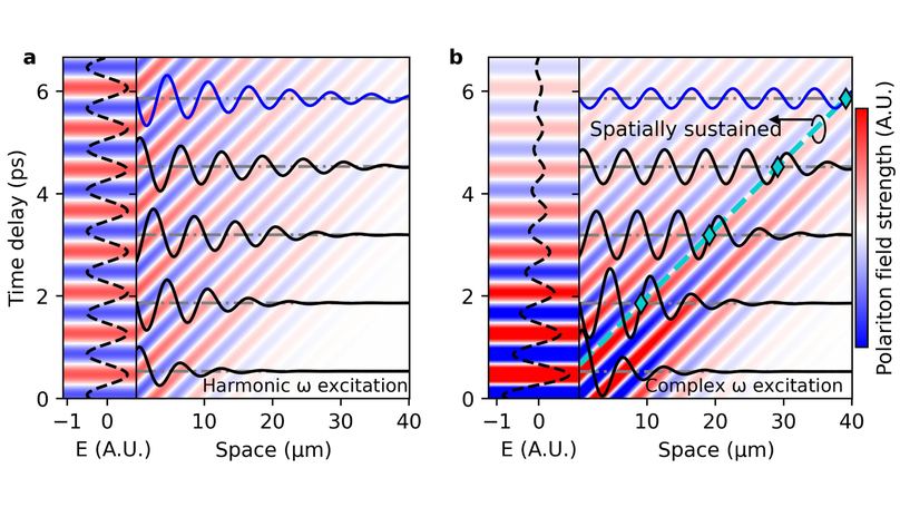
The spatial and temporal dynamics of wave propagation are intertwined. A common manifestation of this duality emerges in the spatial and temporal decay of waves as they propagate through a lossy medium. A complete description of the non-Hermitian wave dynamics, capturing temporal and spatial decays, necessitates the use of complex-valued frequency and/or wavenumber eigen-values. Here, we demonstrate that the propagation of polaritons – hybrid light-matter quasiparticles – can be broadly controlled in space and time by temporally shaping their photonic excitation. Using time-domain terahertz near-field nanoscopy, we study plasmon polaritons in bilayer graphene at sub-picosecond time scales. Suppressed spatial decay of polaritons is implemented by temporally engineering the excitation waveform. Polaritonic space-time metrology data agree with our dynamic model. Through the experimental realization and visualization of polaritonic space-time duality, we uncover the effects of the spatio-temporal engineering of wave dynamics; these are applicable to acoustic, photonic, plasmonic, and electronic systems.
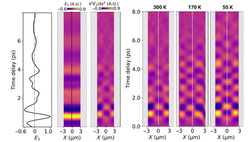
Ultraclean graphene at charge neutrality hosts a quantum critical Dirac fluid of interacting electrons and holes. Interactions profoundly affect the charge dynamics of graphene, which is encoded in the properties of its electron-photon collective modes: surface plasmon polaritons (SPPs). Here, we show that polaritonic interference patterns are particularly well suited to unveil the interactions in Dirac fluids by tracking polaritonic interference in time at temporal scales commensurate with the electronic scattering. Spacetime SPP interference patterns recorded in terahertz (THz) frequency range provided unobstructed readouts of the group velocity and lifetime of polariton that can be directly mapped onto the electronic spectral weight and the relaxation rate. Our data uncovered prominent departures of the electron dynamics from the predictions of the conventional Fermi-liquid theory. The deviations are particularly strong when the densities of electrons and holes are approximately equal. The proposed spacetime imaging methodology can be broadly applied to probe the electrodynamics of quantum materials.
Recent Publications
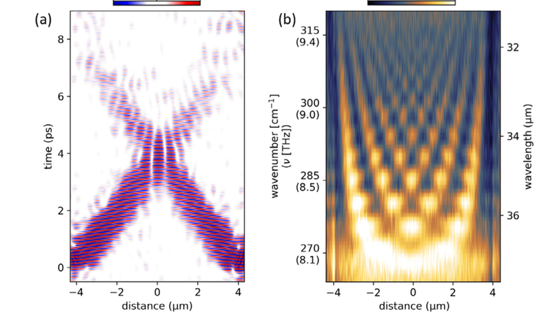
Guiding, storing, and processing light at the nanoscale hinges on understanding how polaritons — hybrid quasiparticles of light and matter — propagate and interfere in both space and time. This work introduces a synchrotron-based technique, SYnchrotron SpaceTimE Mapping (SYSTEM), which captures real-time evolution of polariton wave packets with ∼10 nm spatial and sub-100 fs temporal resolution across an ultrabroadband 5–50 THz range. Here, SYSTEM directly visualizes the creation, interference, and decay of multiple high-quality Fabry-Pérot phonon polariton cavity modes in an α-MoO3 microcavity. These real-space, real-time observations reveal wave-packet dynamics and cavity resonances with record-high quality factors (Q ≈ 100) in the single-digit terahertz regime near 9 THz. SYSTEM thus offers a powerful and broadly applicable platform for probing and engineering ultraslow, deeply subwavelength polaritons, opening new avenues for tailoring light–matter interactions and advancing next-generation THz nanophotonic technologies.
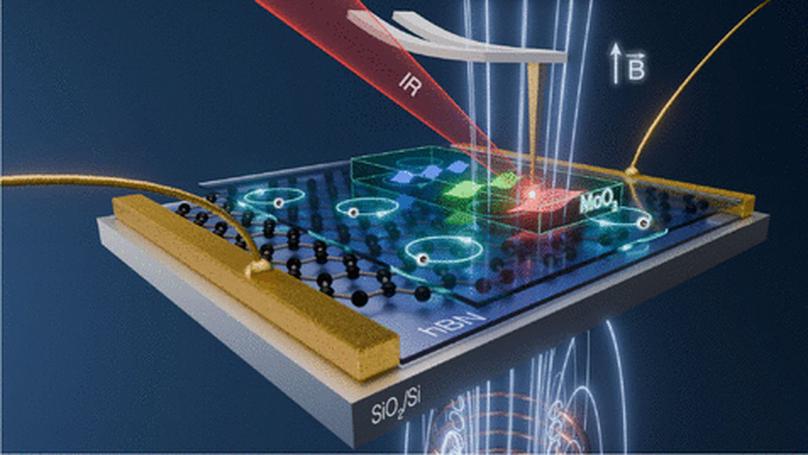
Nanophotonic cavities are the foundation for a broad spectrum of applications, including quantum sensing, on-chip communication, and cavity quantum electrodynamics. In van der Waals (vdW) materials, these cavities can harness polaritons, which are quasiparticles emerging from photon interactions with excitons, plasmons, or phonons that are confined in microscopic sample flakes. Hybrid phonon–plasmon cavities leverage the long lifetimes of phonons and good tunability of plasmons, but their reconfigurability remains fundamentally limited. Here, we introduce a magnetic-field-tuning mechanism for polaritonic cavities in a vdW heterostructure. Specifically, we demonstrate that the primary Landau transition in magnetized charge-neutral graphene can be harvested for controlling polaritonic cavity modes in a graphene-based phononic heterostructure. Additionally, we predict a magnetic-field-induced topological transition in the polariton isofrequency contour, causing a nontrivial cavity mode profile redistribution. Our study underscores the versatility of Landau-based nanophotonic cavities, offering new paradigms for the design and manipulation of light–matter interactions at the nanoscale.
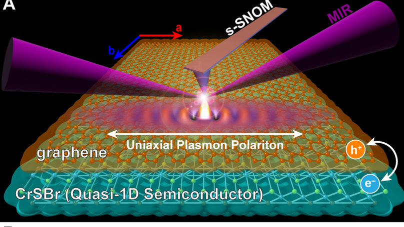
Graphene is a privileged 2D platform for hosting confined light-matter excitations known as surface plasmon-polaritons (SPPs), as it possesses low intrinsic losses with a high degree of optical confinement. However, the inherently isotropic optical properties of graphene limit its ability to guide and focus SPPs, making it less suitable than anisotropic elliptical and hyperbolic materials as a platform for polaritonic lensing and canalization. Here, we present the graphene/CrSBr heterostructure as an engineered 2D interface that hosts highly anisotropic SPP propagation over a wide range of frequencies in the mid-infrared and terahertz. Using a combination of scanning tunneling microscopy (STM), scattering-type scanning near-field optical microscopy (s-SNOM), and first-principles calculations, we demonstrate mutual doping in excess of 1013 cm−2 holes/electrons between the interfacial layers of graphene/CrSBr heterostructures. SPPs in graphene activated by charge transfer interact with charge-induced anisotropic intra- and interband transitions in the interfacial doped CrSBr, leading to preferential SPP propagation along the quasi-1D chains that compose each CrSBr layer. This multifaceted proximity effect both creates SPPs and endows them with anisotropic transport and propagation lengths that differ by an order-of-magnitude between the two in-plane crystallographic axes of CrSBr.
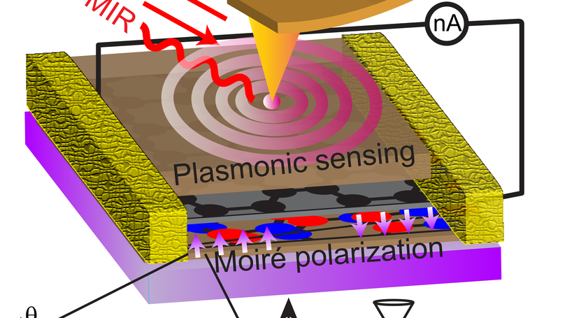
Plasmon polaritons are formed by coupling light with delocalized electrons. The half-light and half-matter nature of plasmon polaritons endows them with unparalleled tunability via a range of parameters, such as dielectric environments and carrier density. Therefore, plasmon polaritons are expected to be tuned when in proximity to polar materials since the carrier density is tuned by an electrostatic potential; conversely, the plasmon polariton response might enable the sensing of polarization. Here, we use infrared nano-imaging and nano-photocurrent measurements to investigate heterostructures composed of graphene and twisted hexagonal boron nitride (t-BN), with alternating polarization in a triangular network of moiré stacking domains. We observe that the carrier density and the corresponding plasmonic response of graphene are modulated by polar domains in t-BN. In addition, we demonstrate that the nanometer-wide domain walls of graphene moirés superlattices, created by the polar domains of t-BN, provide momenta to assist the plasmonic excitations. Furthermore, our studies establish that the plasmon of graphene could function as a delicate sensor for polarization textures. The evolution of polarization textures in t-BN under uniform electric fields is tomographically examined via plasmonic imaging. Strikingly, no noticeable polarization switching is observed under applied electric fields up to 0.23 V/nm, at variance with transport reports. Our nano-images unambiguously reveal that t-BN with triangular domains acts like a ferrielectric, rather than ferroelectric claimed by many previous studies.
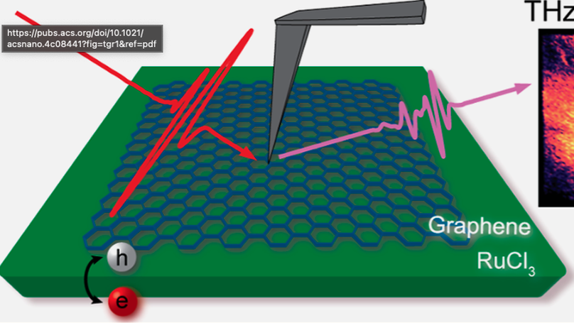
Surface plasmon polaritons (SPPs) provide a window into the nano-optical, electrodynamic response of their host material and its dielectric environment. Graphene/α-RuCl3 serves as an ideal model system for imaging SPPs since the large work function difference between these two layers facilitates charge transfer that hole dopes graphene with n ∼ 1013 cm–2 free carriers. In this work, we study the emergent THz response of graphene/α-RuCl3 heterostructures using our home-built cryogenic scanning near-field optical microscope. Using phase-resolved imaging, we clearly observe long wavelength, heavily damped THz SPPs in a series of variable-size graphene cavities. From this, we extract the plasmonic wavelength and scattering rate in the graphene/α-RuCl3 heterostructures. We determine that the measured plasmon wavelength and electronic scattering rate match our heterostructures’ theoretically predicted values. Our results demonstrate that shaping graphene into bespoke cavity structures enables observation and quantification of SPPs in heavily doped graphene that are largely not addressable with other experimental techniques. Moreover, the manifest lack of metallicity observed in the adjacent doped α-RuCl3 layer provides significant constraints on the nature of the interfacial charge transfer in this 2D heterostructure.
Recent & Upcoming Talks
Contact
- sx2277@columbia.edu
- 888 888 88 88
- 538 WEST 120TH STREET, New York, NY 10463
- Enter Building 1 and take the stairs to Office 200 on Floor 2
-
Monday 10:00 to 13:00
Wednesday 09:00 to 10:00 - Book an appointment
- DM Me
- Skype Me
- Chat on Keybase
- Discuss on Forum

